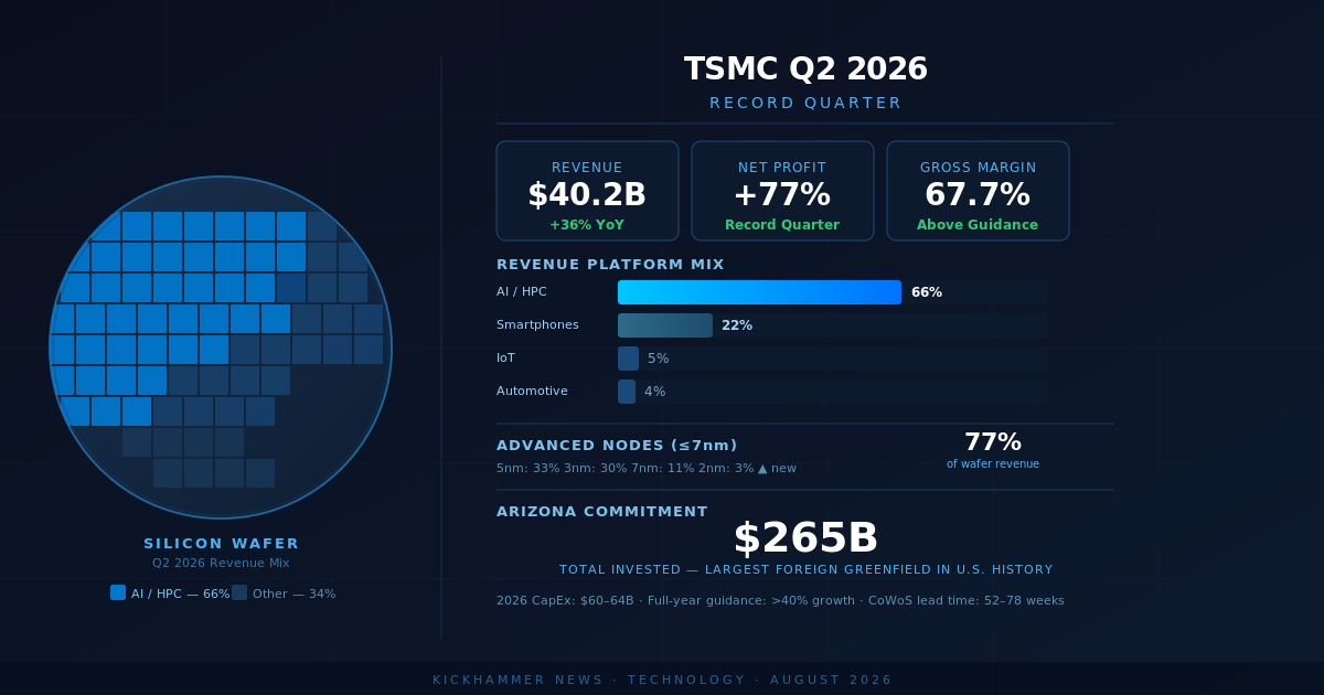
Taiwan Semiconductor Manufacturing Company delivered the most profitable quarter in its 38-year history last month, posting $40.2 billion in revenue for Q2 2026 — a 36% jump year over year — and raising its full-year growth outlook to above 40% for the second time in a single year. Net profit surged 77.4% to NT$706.56 billion. Gross margin hit 67.7%, edging above the company’s own guidance ceiling. And through all of it, management’s primary concern was not whether demand would hold. It was whether TSMC could physically build chips fast enough to meet it.
That constraint — supply, not demand — is the story underneath the record numbers. And it explains a great deal about what is happening to technology prices, AI capability timelines, and the semiconductor industry’s geography right now.
Two-Thirds of the World’s Largest Foundry Is Now AI
The most striking figure from TSMC’s Q2 earnings presentation was not in the revenue or profit lines. It was in the platform breakdown. High-Performance Computing — TSMC’s category for AI accelerators, data center processors, and the GPUs inside gaming PCs — grew 20% in a single quarter and now accounts for 66% of total wafer revenue. Smartphones, which generated the largest share of TSMC’s revenue as recently as 2022, fell to 22%.
For a company whose business model was long defined by Apple’s iPhone orders, a two-thirds-to-one-fifth split represents a fundamental transformation. TSMC is no longer primarily a smartphone foundry that also makes AI chips. It is an AI infrastructure company that also makes smartphone chips. That distinction matters because the two businesses have very different demand profiles: smartphone shipments are tied to consumer sentiment and upgrade cycles; AI accelerator demand is driven by capital expenditure decisions at a handful of hyperscale cloud providers that have shown no sign of slowing down.
The node mix tells the same story. TSMC’s 5-nanometer process accounted for 33% of wafer revenue in Q2; 3-nanometer contributed 30%; and 7-nanometer added 11%. Together, chips at 7nm and below represented 77% of everything TSMC sold — a concentration of value at the leading edge that reflects both how thoroughly AI has skewed demand toward the most advanced processes and how thoroughly TSMC has consolidated its position as the only company capable of manufacturing them at scale.
2nm: A New Transistor Architecture Enters Production
Q2 2026 also marked the first meaningful commercial revenue contribution from TSMC’s 2-nanometer process node, designated N2, which accounted for 3% of wafer revenue as the company completed the transition from engineering samples to paying production.
N2 represents the most significant architectural change in transistor design in more than a decade. Every chip TSMC has ever manufactured for commercial customers — from early 500nm processes through the 3nm node that produces NVIDIA’s current Blackwell GPUs — has relied on a FinFET transistor: a vertical silicon fin with a gate electrode wrapped around three sides. N2 replaces this with a gate-all-around nanosheet transistor, in which three horizontal silicon ribbons are fully encircled by the gate on all four sides.
The engineering significance is not cosmetic. In a FinFET, the three-sided gate leaves one side of the channel exposed, creating a leakage pathway — a current that flows even when the transistor is supposed to be off — that worsens as the fin shrinks. The four-sided gate of a nanosheet transistor eliminates that pathway entirely. The result, according to TSMC’s specifications: N2 delivers 15% faster switching speed, or 30% lower power consumption at the same speed, compared to N3, while improving transistor density by more than 15%. On-chip memory density improves by 11%, compared to a 6% gain when N3 was introduced — a jump that TSMC engineers attribute directly to the new architecture.
The tradeoff is a steeper yield ramp. Manufacturing a new transistor geometry from scratch takes longer to achieve consistent production yields than extending a FinFET process optimized over more than a decade. CFO Wendell Huang told analysts that the steep production increase expected in the second half of 2026 will dilute gross margins by approximately 3 to 4 percentage points before scale efficiencies take hold. For Q3 2026, TSMC guided revenue of $44.6 billion to $45.8 billion — roughly 37% year-over-year growth at the midpoint — with margins expected to ease to 65%–67%.
CoWoS: The Bottleneck Above the Bottleneck
If advanced chip fabrication is the constraint that most people understand, CoWoS packaging has become the constraint that most people miss — and TSMC’s Q2 results confirmed it is now the tighter of the two.
CoWoS — Chip-on-Wafer-on-Substrate — is the technology that physically integrates AI chips with high-bandwidth memory. It places the AI logic die and multiple stacks of HBM memory side by side on a silicon interposer: a flat silicon wafer fabricated with dense copper interconnects called Through-Silicon Vias. Inter-die signals travel microns through silicon rather than millimeters through circuit board material, increasing memory bandwidth from roughly 1 terabyte per second (GDDR6) to more than 3 terabytes per second (HBM3E). Every NVIDIA Blackwell GPU, every AMD MI-series accelerator, and every custom AI chip from Google, Amazon, and Microsoft depends on CoWoS for that bandwidth. There is no alternative packaging platform at comparable yield for AI accelerator workloads.
TSMC confirmed this quarter that CoWoS capacity is fully booked, with lead times extending 52 to 78 weeks. Manufacturing a CoWoS interposer requires a dedicated silicon fabrication step — the interposer is itself a wafer, produced in TSMC’s advanced packaging fabs with its own process steps, equipment, and yield curve. As AI chips advance and each new generation requires more HBM stacks per die to feed larger models, demand for CoWoS capacity increases alongside — or faster than — demand for the chips themselves. CEO C.C. Wei acknowledged that the packaging bottleneck is constraining customer delivery timelines and said TSMC welcomes competitive packaging offerings from rivals, framing them as relief for an oversubscribed market rather than a competitive threat.
Competitors including Intel and Samsung have equivalent architectures, but independent assessments place them two to three years behind TSMC in production volume and yield for AI accelerator workloads.
$265 Billion Committed to Arizona — and Counting
Beyond the quarter’s operating results, the most consequential disclosure was TSMC’s capital allocation plan. The company raised its 2026 CapEx budget to $60–64 billion, up from an earlier range of $52–56 billion — an increase of up to $12 billion in a single quarter. Between 70% and 80% of that spending will flow to advanced process technologies, with the remainder split between specialty nodes and advanced packaging.
TSMC also announced an additional $100 billion investment in its Arizona manufacturing operations, encompassing four or more additional fabs covering both front-end wafer fabrication and advanced packaging for 2nm-class and below technologies. Total committed investment in Arizona now stands at approximately $265 billion — up from $165 billion announced in March 2025 — representing the largest foreign direct investment in a greenfield manufacturing project in American history.
Wei was direct about the timeline: “The CapEx in the next three years will be even more significantly higher than the past three years.” The Arizona expansion is simultaneously TSMC’s most ambitious geographic commitment and its most visible acknowledgment that supply constraints, rather than demand uncertainty, are the binding limit on its own growth.
Agentic AI Opens a Second Demand Channel
Management also flagged a structural development that has not yet fully registered in infrastructure discussions: the rise of agentic AI is changing the composition of data center demand in ways that benefit TSMC beyond its existing GPU business.
In the chatbot era — roughly 2022 through mid-2025 — AI demand was dominated by GPU-centric model training and inference, with CPUs serving short orchestration bursts. In agentic AI architectures, AI systems autonomously execute multi-step tasks: browsing, writing, coding, communicating, and making decisions with minimal human prompting. These workloads require sustained, always-on CPU processing for tool calling, memory management, API orchestration, and multi-step reasoning loops. Independent analysis suggests agentic applications may require four times as many CPU cores per gigawatt of data center power as training-era infrastructure — shifting the CPU-to-GPU deployment ratio from a historical 1:8 toward 1:1 for some workloads.
TSMC manufactures leading chips across every major CPU architecture — x86 (Intel, AMD), Arm, and RISC-V — and Wei said the company is already working with CPU customers to allocate capacity for agentic AI applications. This creates incremental silicon demand layered on top of the existing GPU-accelerator wave, not a substitution for it.
What TSMC’s Numbers Mean for Everyone Else
TSMC’s quarterly results carry analytical weight well beyond a single company’s financials. Because TSMC manufactures the GPU dies inside virtually every AI accelerator from NVIDIA and AMD, as well as custom AI silicon for Google, Apple, Amazon, and Microsoft, its revenue trajectory provides a cleaner real-time read on actual AI chip purchasing behavior than the capital expenditure announcements of cloud providers — which capture commitments, not deliveries.
By that measure, the Q2 report is unambiguous. Revenue growth accelerated to 36% year-over-year. The full-year outlook rose from above 30% to above 40%. CapEx was raised twice in a single year. And the CEO extended his previously stated five-year AI semiconductor compound annual growth rate — already described as “in the mid-to-high 50s” — with the assessment that the underlying trend is “stronger and stronger.”
For consumers, the implications are more immediate and less abstract. The shortages of AI accelerators, the rationing of high-bandwidth memory, and the upward pressure on graphics card prices all trace back to the same root cause: AI buyers are outbidding consumer hardware for wafers, memory, and packaging capacity. When two-thirds of the world’s most advanced foundry is committed to HPC and still cannot build fast enough to stop margins from climbing, the squeeze on everything else is not a temporary blip. TSMC’s numbers say it is the new baseline — at least until fabs that haven’t been built yet begin shipping wafers, which will not happen this year, or next.
The silicon needed to power the AI buildout remains, for now, the binding constraint on everything else. And the packaging step that integrates that silicon with memory is an even tighter constraint than the silicon itself.