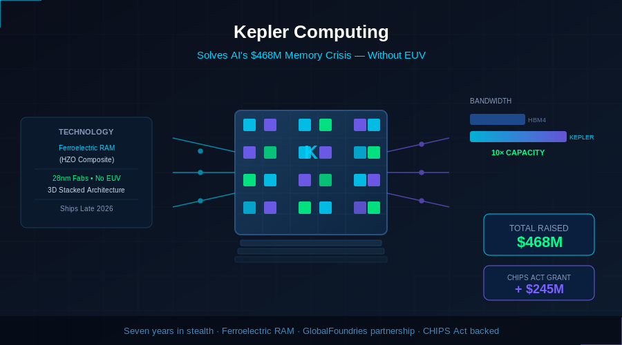
A San Jose startup claims it cracked the AI memory bottleneck without the $150M machines everyone else depends on — and it has $468M in venture funding and CHIPS Act backing to prove it.
For seven years, Kepler Computing operated in near-total silence out of San Jose, California. No press releases. No conference talks. Just a small team of materials scientists and chip engineers running test after test on ferroelectric compounds, trying to crack a problem that has quietly become one of the most expensive constraints in artificial intelligence: memory.
This week, Kepler stepped out of stealth with $468 million in late-stage venture funding and a bold claim — that it has found a way to build AI memory chips that are faster, denser, and more energy-efficient than today’s high-bandwidth memory, without relying on the Extreme Ultraviolet lithography machines that cost upward of $150 million apiece and can’t be ordered fast enough to keep up with AI’s appetite.
The Memory Wall Nobody Talks About
Every AI model you interact with today runs into the same invisible ceiling. Compute gets faster every generation. Nvidia’s GPUs improve dramatically. But memory — specifically the speed at which data can move between storage and the processor — hasn’t kept pace. The industry calls this the “memory wall,” and for AI training and inference workloads, it’s becoming increasingly expensive to work around.
High-bandwidth memory, or HBM, was supposed to be the answer. SK Hynix, Samsung, and Micron all produce it, and it offers significantly better performance than conventional DRAM. The problem is that all three producers are sold out through at least late 2026, with production capacity locked up by hyperscalers pouring billions into AI infrastructure. DRAM prices jumped 58% to 63% quarter-over-quarter in Q2 2026 alone, according to TrendForce. NAND flash prices followed with a 70% to 75% spike in the same period.
Kepler’s argument is that the HBM market doesn’t just have a supply problem — it has a physics problem. And their solution is built from different materials entirely.
Ferroelectric RAM, Reimagined
Rather than continuing to shrink transistors through EUV lithography, Kepler’s engineering team took a different path. After testing 35 distinct iterations of a proprietary ferroelectric composite material, the company landed on a hafnium zirconium oxide-based formulation that allows it to store and access data at speeds competitive with high-speed SRAM while offering up to 10 times the memory capacity of standard SRAM and HBM configurations.
The key breakthrough is that Kepler’s technology works on existing 28-nanometer fabrication lines — mature fabs that chipmakers have largely depreciated and run at lower cost than cutting-edge nodes. By layering its ferroelectric materials onto these existing processes using 3D stacking techniques, Kepler says it can achieve densities normally associated with 2-nanometer or 3-nanometer chips, without touching an EUV machine.
In practical terms, Kepler claims to have converted a mature 28nm fab line into a working memory plant in eight months — compared to the two to three years a new-build facility would require. The resulting architecture promises energy efficiency and bandwidth-per-watt performance that the company says can compete with high-speed SRAM at scale.
Peer-reviewed research published in April 2026 demonstrated that Kepler’s architecture can be manufactured using conventional CMOS processes, lending some independent credibility to the technical claims. Whether the results hold up at production volumes is the critical question the company has yet to fully answer.
Who’s Betting $468 Million on This
The funding round drew a notable mix of strategic and financial investors. GlobalFoundries committed $50 million and is serving double duty as both a financial backer and the primary manufacturing partner — testing Kepler’s technology at its Vermont facility and in Singapore. Intel Capital and AMD Ventures both participated, meaning two of the three major x86 chip companies have money on this bet. Baillie Gifford and Gates Frontier rounded out the major backers.
The strategic logic for Intel Capital and AMD Ventures isn’t hard to follow. Both companies sell AI accelerators that share the same HBM shortage their customers are experiencing. Any technology that meaningfully expands the supply of high-performance AI memory — or displaces HBM with something cheaper — changes the competitive dynamics around their own chips.
GlobalFoundries’ role deserves particular attention. The company doesn’t operate EUV lines and has largely ceded the leading-edge foundry race to TSMC and Samsung. Kepler’s EUV-free approach fits neatly into GlobalFoundries’ existing capabilities, and a commercial success here would give GlobalFoundries a meaningful stake in the AI memory market without requiring a multi-billion-dollar upgrade to its fab infrastructure.
Federal Money, Federal Stakes
Alongside the private raise, the U.S. Department of Commerce issued a letter of intent in July 2026 to provide up to $245 million in CHIPS Act funding to Kepler — earmarked specifically for research and development of high-performance AI memory. As a condition of the federal investment, Kepler agreed to grant the U.S. government a minority, non-controlling equity stake in the company.
This structure — federal cash in exchange for equity rather than loans or grants — reflects a policy direction that’s grown more common under CHIPS Act implementation, as the government seeks to retain upside in the companies it funds. The Cato Institute noted the arrangement as part of a broader trend toward government ownership stakes in chip companies, describing it as “becoming routine” under current policy.
For Kepler, the $245 million adds to the $468 million private raise, putting total available capital somewhere north of $700 million — enough to fund both Singapore production scale-up and the beginnings of a U.S. manufacturing footprint.
The Road to Production
Kepler’s stated timeline: first AI memory samples ship in late 2026, volume production ramps at GlobalFoundries’ Singapore plant in 2027, and U.S. manufacturing begins in 2028. The 2027 Singapore production allocation is reportedly already finalized, which gives the timeline at least some external validation.
The closer obstacle is proving that the technology works at scale, not just in a lab or on a converted test line. Kepler’s materials have been tested in controlled conditions by a team that clearly knows what it’s doing — co-founder and CTO Sasi Manipatruni previously served as founding director of Intel’s FEINMAN research center and co-invented MESO spin-orbit logic. CEO Debo Olaosebikan holds a physics PhD from Cornell and sits on the U.S. Department of Commerce’s Industrial Advisory Committee. This isn’t a team that stumbled into semiconductors.
But the history of memory technology is littered with promising materials that couldn’t scale. Phase-change memory, resistive RAM, magnetoresistive RAM — all of these approaches showed laboratory promise and faced severe challenges in high-volume manufacturing. Ferroelectric RAM is not new; versions of FeRAM have existed for decades in niche applications. Kepler’s specific innovation is in the materials engineering and 3D stacking approach that it claims finally makes FeRAM competitive with HBM at scale.
What It Means for AI Infrastructure
If Kepler’s technology works as described, the implications ripple well beyond chip pricing. Data center operators currently plan AI infrastructure deployments around the assumption that HBM will be constrained and expensive for years. A credible alternative supplier — especially one that can use existing fab capacity — would fundamentally shift that calculus.
It would also put pressure on SK Hynix, Samsung, and Micron to accelerate HBM4 timelines and potentially lower pricing. The incumbents are already pouring billions into next-generation HBM capacity. Kepler’s emergence doesn’t threaten their market overnight, but it creates a competitive pressure that didn’t exist six months ago.
For Nvidia, which depends heavily on SK Hynix’s HBM production for its highest-end AI training chips, a healthy alternative memory ecosystem would reduce supply-chain risk and potentially allow it to ship more GPUs faster. The broader AI buildout is arguably supply-constrained more by memory than by compute at this point — a problem Kepler, if it delivers, is precisely positioned to address.
Seven years of materials science, $468 million in backing, and a $245 million federal commitment have finally come into public view. Whether Kepler can turn its lab results into production-ready AI memory at scale is a question 2027 will answer. But the AI industry’s memory crisis is real, the incumbents are locked up, and Kepler just introduced itself as the first serious alternative.
Sources: [Hoodline](https://hoodline.com/2026/09/san-jose-startup-kepler-nabs-468m-to-break-ai-s-costly-memory-bottleneck/), [XenoSpectrum](https://xenospectrum.com/en/kepler-ferroelectric-ai-memory/), [Overclock3D](https://overclock3d.net/news/memory/kepler-aims-to-end-the-ai-memory-crisis-with-custom-memory-tech/), [Superintelligence News](https://superintelligencenews.com/companies/ai-memory-bottleneck-kepler-468m-bet/)