August 4, 2026
For half a century, the semiconductor industry ran on a single north star: pack more transistors onto a chip. Moore’s Law — Gordon Moore’s 1965 observation that transistor density would double roughly every two years — became both a business forecast and a cultural religion for Silicon Valley and Hsinchu alike. But a gathering of semiconductor engineers and researchers in Taipei yesterday made one thing clear: the transistor era as the primary competitive battlefield is ending, and AI is the force pulling the industry into what comes next.
At the Taiwan-Japan Semiconductor Technology Forum, experts from leading chipmakers and research institutions delivered a remarkably consistent message: artificial intelligence has outrun what conventional transistor scaling can deliver. The new competition will be won not by those who can shrink silicon the fastest, but by those who can integrate entire systems — computing, sensing, power management, memory, and optical communication — into unified packages that behave as one.
Moore’s Law Meets Its Wall
Tsai Hann-huei, deputy director-general of Taiwan’s Semiconductor Research Institute (TSRI), put the situation bluntly. “Advances in process-node technology are slowing while AI-driven demand for bandwidth continues to surge,” Tsai told the forum. “Leadership will come from system-level co-optimization, not transistor scaling alone.”
The numbers back him up. A modern AI training cluster consumes hundreds of megawatts and connects thousands of accelerators that must exchange data at terabit-per-second speeds. Squeezing another few billion transistors onto a die simply cannot solve the bandwidth, power, and latency problems that define today’s AI infrastructure challenge. The bottleneck has moved from computation to communication — from inside the chip to between chips, and between chips and memory.
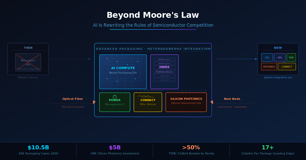
This is why the industry has pivoted hard toward advanced packaging: the art of assembling multiple chiplets, dies, and components into a single package that behaves as if it were one monolithic chip. Heterogeneous integration — combining logic, memory, analog circuits, and optical components from different manufacturers and process nodes — has become the defining technical challenge of the decade.
The New Competitive Battleground
Dinos Huang, senior director of corporate research and development at ASE Technology Holding — the world’s largest semiconductor packaging and testing company — framed it with the directness of someone who has spent decades watching where pressure in the supply chain actually sits. “Hardware is becoming the new bottleneck,” he told the forum.
As AI models have grown from billions to trillions of parameters, and as inference workloads have migrated from data centers to edge devices — AI glasses, autonomous vehicles, humanoid robots, drones — the demands on packaging have become almost brutal. Greater bandwidth means more signal traces. More computing power means more heat. Tighter latency requirements mean shorter physical distances between components. Structural stability matters when a package containing hundreds of billions of transistors gets installed in a car or strapped to a robot’s back.
ASE’s response has been aggressive. Last week the company raised its 2026 capital expenditure to $10.5 billion, a 23.5% increase from its prior $8.5 billion plan. About 70% of that increase flows toward capacity expansion for LEAP — Leading-Edge Advanced Packaging. The company expects LEAP revenue to exceed $3.5 billion this year alone.
It is also moving from wafer-level to panel-level packaging, a shift analogous to moving from small canvases to large ones: more usable area, better material utilization, and critical when AI accelerators keep growing in physical footprint.
Silicon Photonics: Light Replaces Wire
Perhaps the most consequential shift on the horizon is the move from electrical to optical interconnects. As data rates between chips and systems push into the terabit range, copper wires lose the race — they heat up, attenuate signals, and consume disproportionate power. Light moves faster, loses less, and generates almost no heat in transit.
Silicon photonics — the technology of fabricating optical components on standard silicon wafers — is racing from specialized niche to mainstream data center technology. United Microelectronics Corp (UMC), the world’s fourth-largest contract chipmaker, announced last week that it has already delivered the first mass-produced 12-inch silicon photonics wafers, and it is committing up to $5 billion over the next two to three years to expand that capacity. The company’s CEO Jason Wang expects AI-related revenue to reach $300 million this year and cross $1 billion within three years.
“We actually feel pretty optimistic about advanced packaging,” Wang said at the company’s earnings conference, “and that’s why we started facility deployment.” UMC is positioning silicon photonics and advanced packaging as the core of its growth story — a remarkable pivot for a company historically associated with mature process nodes.
TSRI’s Tsai acknowledged the engineering challenges that make this transition harder than it sounds. Getting heat, electricity, optics, and mechanical stress to coexist peacefully inside a single tightly packed package requires a level of cross-disciplinary expertise that no company can master alone. Progress will require partnerships among chipmakers, equipment suppliers, materials scientists, academic institutions, and government research bodies — precisely the kind of collaboration the Taiwan-Japan forum was designed to accelerate.
The Race for Packaging Capacity
The urgency is already visible in capacity data. Nvidia has reportedly booked more than half of TSMC’s CoWoS (Chip on Wafer on Substrate) advanced packaging capacity for 2026 and 2027, leaving competitors scrambling for alternatives. AMD, Google, Amazon, and a growing roster of AI ASIC developers must secure packaging capacity while simultaneously managing the design complexity of assembling four, eight, or even seventeen chiplets into a single package without unacceptable performance penalties.
The interposer supply chain — the intermediary layers that connect chiplets inside a package — has become a choke point almost as consequential as chip fabrication itself. TSMC, Samsung, and Intel hold dominant patent positions, but new entrants, particularly from China, are accelerating fast. At July’s WAIC 2026 conference in Shanghai, Enflame Technology and Shanghai Xianfeng Technology jointly demonstrated China’s first CoPoS (Chip on Package on Substrate) advanced packaging sample with a glass substrate for AI computing chips — a signal that the competition for packaging supremacy is global.
Beyond the Data Center
The applications driving these investments are not limited to hyperscale AI training. Tsai’s forum presentation highlighted a telling list: automobiles, humanoid robots, AI glasses, drones. Each of these devices requires semiconductor systems that combine computing, sensing, power management, and connectivity in packages that are small, rugged, and efficient enough to operate away from controlled data center environments.
This means the packaging revolution is not a niche trend for AI chip manufacturers — it is a platform shift that will touch nearly every product category. A humanoid robot’s perception system, an autonomous vehicle’s sensor fusion unit, a pair of AI glasses that can understand the world in real time — all of these require the kind of heterogeneous integration that the industry is now racing to master.
A New Industry Hierarchy
The implications for competitive dynamics are profound. For decades, the semiconductor industry hierarchy was clear: the leading foundry (TSMC, then Samsung) that could print the smallest transistors held the highest ground. Advanced packaging changes that calculus.
A company that cannot access the latest 2nm process node but masters heterogeneous integration, silicon photonics, and panel-level packaging may be able to deliver AI systems that outperform chips built on nominally superior processes. The barriers to entry are different — they involve materials science, thermal engineering, optical design, and test infrastructure as much as lithography — and they are ones that a wider range of companies can compete on.
This is not a comfortable realization for every incumbent, but it creates genuine opportunity for companies like UMC, ASE, and a cohort of specialized packaging and materials firms that have spent years building expertise in exactly the capabilities the AI era now demands.
The transistor is not dead — TSMC’s 2nm and beyond roadmap still matters enormously, and chip density will keep climbing. But transistor count alone can no longer define the winner. In the AI era, the semiconductor industry’s crown goes to whoever can put all the pieces together.
Sources: Taipei Times, Taiwan-Japan Semiconductor Technology Forum (August 3, 2026); UMC Q2 2026 earnings (July 29-30, 2026); ASE Technology Holding Q2 2026 earnings (July 31, 2026)