At the World Manufacturing Convention in Hefei this morning, ChangXin Memory Technologies made an announcement that the global semiconductor industry had been bracing for: its fifth-generation DRAM platform has entered mass production. Two new 24-gigabit LPDDR5X products are already shipping inside Chinese flagship smartphones. And none of it required the advanced lithography machines that US export controls were designed to keep out of China’s hands.
The story of CXMT’s G5 chip is, in many ways, the story of China’s semiconductor strategy in miniature — a tale of patient engineering, state-backed capital, and a willingness to build around the walls Washington has erected rather than through them.
What the G5 Platform Is
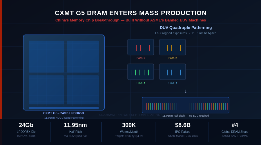
The G5 DRAM process achieves an active-area half-pitch of 11.95 nanometers. To put that in context, that figure puts CXMT within striking distance of the sub-12nm nodes that Samsung and SK Hynix have been operating at in recent years — the tier of DRAM that powers flagship smartphones and high-performance computing applications.
The trick CXMT’s engineers used to get there is called quadruple patterning. Extreme ultraviolet (EUV) lithography — the kind produced exclusively by ASML in the Netherlands, and banned for export to China under US and Dutch controls — achieves fine circuit features using 13.5-nanometre wavelength light in a single exposure. CXMT instead runs four aligned deep-ultraviolet (DUV) exposures to carve the same dimensions, each pass inscribing part of the circuit pattern that EUV would produce in one shot.
The engineering challenge is keeping those four exposures aligned closely enough that their errors don’t compound. At sub-12nm dimensions, misalignment errors are catastrophic — they destroy yield. CXMT’s claim that the G5 achieves at least 50 percent more gross dies per wafer than its fourth-generation predecessor implies its engineers have solved, or sufficiently controlled, that alignment problem. If the yield number is accurate and sustained, it’s a genuine process control achievement.
The 24Gb die size itself is significant. A single G5 LPDDR5X die holds 3 gigabytes — 50 percent more than the 16Gb (2GB) dies that defined the previous generation. For smartphone manufacturers, that means denser, more capable memory in the same physical footprint. For CXMT, it means more memory per wafer and better economics at scale.
The Company Behind the Chip
CXMT — formally ChangXin Memory Technologies — was founded in 2016 in Hefei, the capital of Anhui province and one of China’s designated semiconductor development hubs. The company started from scratch with no established process technology, no significant customer base, and a memory market dominated by three entrenched giants: Samsung Electronics, SK Hynix, and Micron Technology.
Six years later, it was producing 40,000 wafers per month. As of September 2026, that figure has grown to approximately 300,000 wafers per month across its facilities in Hefei and Beijing, and the company is targeting 350,000 to 375,000 wafers monthly by year-end. That trajectory — from startup to fourth-largest DRAM producer globally in a decade — has no obvious parallel in the history of semiconductor manufacturing.
The July 2026 IPO on Shanghai’s STAR Market added another chapter to that story. CXMT raised approximately $8.6 billion at 212 times oversubscription — a level of domestic investor enthusiasm that reflects both the strategic importance Chinese markets assign to semiconductor self-sufficiency and the genuine confidence that CXMT’s production numbers had earned. The IPO briefly triggered a sharp sell-off in Micron and SK Hynix shares, as markets digested what a fourth credible DRAM competitor could mean for pricing.
A multi-year supply agreement with Tencent, valued at roughly $3 billion, provided another signal: China’s largest technology platform had decided to anchor part of its memory supply chain in CXMT rather than continue to rely on the trio of foreign suppliers that export controls could, in theory, be used to pressure.
What “World’s Fourth-Largest” Actually Means
CXMT’s claim to fourth-largest global DRAM market share requires some unpacking. The three incumbents — Samsung, SK Hynix, and Micron — together hold somewhere between 90 and 95 percent of the market. The remaining fraction has historically been divided among a handful of smaller players, most of them not producing leading-edge DRAM at all. CXMT’s positioning as number four is real, but the gap between fourth and third is still measured in tens of billions of dollars in annual revenue.
Where CXMT’s scale is most tangible is in the domestic Chinese market. Chinese smartphone brands integrating CXMT’s LPDDR5X did not wait for independent process verification before shipping handsets. The phones exist. The chips are running in them. The output is real in a way that CXMT’s process claims, which have not been verified by independent foundry analysis, are not yet.
The distinction matters for how to read the G5 announcement. CXMT Vice President Luo Xiaodong told the World Manufacturing Convention that “our process capability is now on par with the most advanced mass-produced nodes out there in the industry.” That comparison was made at a Chinese government-organized industrial forum in Hefei, before an audience of domestic supply-chain partners and state investors. Independent process benchmarking — the kind of third-party analysis that would let an outside engineer confirm the 11.95nm figure against a Samsung or Hynix equivalent — has not yet been published.
The Export Control Calculus
When the United States and its allies moved to cut China off from ASML’s EUV machines several years ago, the underlying assumption was explicit: EUV is necessary for leading-edge DRAM. Without it, Chinese memory manufacturers would plateau somewhere in the 15–20nm range and fall progressively further behind as the industry moved to tighter nodes. The ban, in that framing, was a way of locking in a permanent technology gap.
The G5 announcement tests that assumption at 11.95nm. CXMT has not said whether its DUV quadruple patterning approach can be extended to the 10nm-class processes Samsung and SK Hynix are moving toward. The yield improvement the company is claiming at G5 does not automatically extend to G6. Each shrink brings new alignment challenges that the previous generation’s solutions may not solve.
What the G5 does demonstrate is that the crossover point — where DUV quadruple patterning stops working — has not yet been reached at 11.95nm. Whether it comes at 10nm, 9nm, or somewhere below is an open engineering question that CXMT’s roadmap will eventually answer.
The policy implication is significant. The export control strategy was premised on a technology ceiling. CXMT has moved that ceiling higher. US officials tracking China’s semiconductor progress will need to update their models accordingly — and consider whether additional restrictions on DUV equipment itself, which is already widely distributed in China, would meaningfully slow CXMT’s next-generation development without causing collateral damage to the global supply of those machines.
Impact on the Global Memory Market
For Samsung, SK Hynix, and Micron, the G5 announcement changes the competitive math in specific segments. CXMT’s LPDDR5X targets mid-to-high-end smartphones — a large and price-sensitive market where a credible, cost-competitive fourth supplier has obvious consequences for pricing pressure. Micron, the smallest of the three incumbents, with 22–24 percent global DRAM market share versus Samsung’s 40-plus percent, faces the sharpest exposure: it competes heavily in the mobile DRAM segment, and its margins are thinner than Samsung’s diversified business affords.
The HBM market — high-bandwidth memory used in AI training infrastructure — is a different story. SK Hynix’s HBM3E stack, which powers the majority of AI accelerator systems currently deployed, operates on a product roadmap that CXMT has not published an equivalent for. The G5 LPDDR5X is not an AI training chip. The gap at the leading edge of AI memory has not closed.
What has changed is the competitive baseline. In the smartphone memory market, CXMT is no longer a minor domestic player making chips that Chinese brands use because import alternatives are politically complicated. It is a G5 producer shipping high-performance DRAM that, by CXMT’s own account, competes on process capability with the global leaders.
Looking Ahead
CXMT’s trajectory over the next 18 months will answer several open questions at once. Can it sustain the yield improvement it is claiming at the volume its wafer targets imply? Can it extend the DUV quadruple patterning approach to a subsequent generation? Will the Tencent supply deal and the domestic smartphone integrations translate into the kind of cost-reduction curve that has historically rewarded scale in DRAM manufacturing?
The G5 announcement, made at a government forum in Hefei on a Saturday morning, is not the end of the story. It is the point at which the story’s premise shifted. The export control framework assumed a ceiling that CXMT has not yet hit. The ceiling exists somewhere — the physics of DUV quadruple patterning are not unlimited — but that somewhere is now further away than it was before today’s announcement.
Samsung and Micron shareholders have already noticed. The question for the rest of the industry is how to think about a competitor that built its way to the leading edge without the tools everyone assumed were required to get there.